Preface
To efficiently verify modern Mixed Signal SoC, verification engineers face a myriad of challenges every day. As designs keep getting larger and more complex, it has a profound impact on the verification cycle. This document outlines many of the advance steps one must follow for effectively and efficiently debugging a Mixed Signal SoC. This document can be helpful for AMS verification engineers who want to debug and verify Mixed Signal SoC. For analog and digital verification engineers, this offers the opportunity to peek into, and better understand, the domain of the counterparts and the disciplines that they are not directly responsible, but dependent on the overall success of the Mixed Signal project.
The document is constructed to cover a broad range of debugging steps, which are required for Mixed Signal SoC. While there is, some degree of specificity that increases within the debugging steps described in this document, most of them are self-contained and tackle a specific aspect of Mixed Signal SoC debugging.
Introduction
A Mixed-signal design integrates both analog and digital functionality on the same chip. The interaction between an analog and digital sub-system is the key in the verification of Analog and Mixed Signal Design.
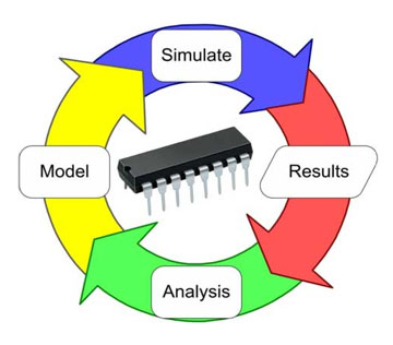
Mixed signal verification and debugging in a typical AMS verification cycle (as shown in Figure1) starts with proper voltage/current level checks of the power pins.

Figure 1 Typical AMS Verification cycle
Common Issues faced during AMS Verification cycle:
Following are the common issues one may encounter during AMS simulation.
- Pin swapped/mismatches between analog IPs when integrated at the analog top level.
- A branch is not properly terminated in a Verilog-AMS model – a modeling issue.
- Simulation takes longer time because of large SPICE design and dump file size
- When a digital signal is driving an analog signal and vice-versa, the signal in one domain (either in digital or in analog) is correct. However, in the other domain it is not showing correct value because of incorrect connect module.
- Improper simulator settings may lead to incorrect results.
- Digital control signals coming to the analog IPs are not matching when verified with analog and digital integrated in a Mixed Signal environment.
- Hierarchical references in digital test bench for signals in analog domain
Following steps show how a Mixed-signal design can be debugged in an effective and efficient way to overcome the aforementioned issues.
Rule 1: Test Bench configuration with SPICE design and Verilog-AMS model in AMS simulation

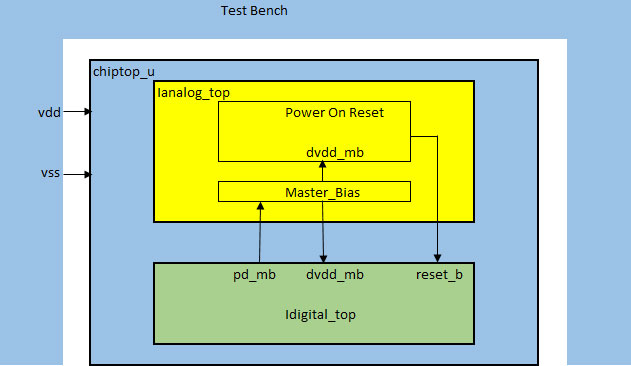
Figure 2 Mixed Signal Design interaction
![]()
Simulation of the entire analog design in a mixed signal design (as shown in Figure 1) can take long time to simulate. Therefore, some effective measures must be taken in order to simulate the analog design in the context of a Mixed Signal SoC. Modeling approach with Verilog-A/MS plays a very important role in improving simulation time.
Figure 2 shows both POR and Master Bias have been used in SPICE for the AMS simulation. We can use different configurations with SPICE and Verilog-AMS model for an effective and efficient Mixed Signal SoC verification. The most critical block in Analog design will be used with SPICE and the lesser critical block can be used with Verilog-A/MS model in AMS simulation. This will help us with improvement in simulation time.
Rule 2: Narrow down the issue in SPICE design during AMS simulation with modeling approach
This can be achieved by modeling approach of the design with Verilog-AMS language. The best way, to resolve any SPICE issue is that, replace the entire design with Verilog-AMS models and then keep one module in SPICE at a time. This will figure out which SPICE subckt is causing the issue.
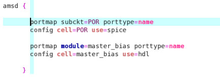
For example, if there is an issue with the analog_top SPICE netlist which includes POR and Master Bias as shown in Figure 2, the best way to resolve which analog block is mainly causing the issue is that, you configure one of the IPs (e.g. Master Bias) in amsd block with Verilog-AMS model and the other IP (e.g. POR) as SPICE as shown below in Figure 3 and check if there is any issue in the analog_top. If the issue is valid, then there is certainly an issue in the POR SPICE netlist.

Figure 3 configuring POR as SPICE and master_bias as hdl
If the issue is vanished then this ensures that there is certainly an issue with the Master Bias SPICE netlist.
This can also be helpful in finding out which part of the design is causing the convergence issue.
Rule 3: Setting up correct Connect module through Connect Rule in AMS simulation
An insertion of wrong connect module in the AMS simulation leads to wrong outputs. Hence, proper care must be taken while setting up Connect Rule.
It is a good practice to use “-iereport” and “-disres detailed” in the irun option for efficient debugging in a typical Cadence Flow. This will generate ams_ieinfo.log file which contains the information about the connect modules inserted in the compile directory.
Connect Rule can be set with the “mode=split” option to improve the accuracy of the simulation. Default option for mode is merge if not specified.
Typical examples of setting up connect rule with “ie” card in the ams configuration file are shown below:

Figure 4 setting up connect rule with ie card
Rule 4: Include correct process corners in SPICE simulation
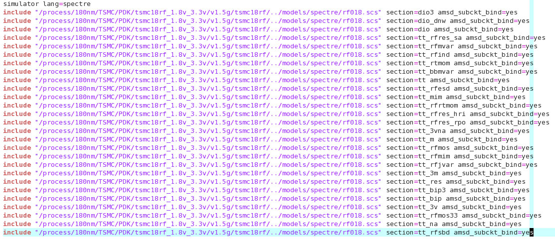
Any SPICE design requires proper device model libraries to be included with the design for its proper functionality. Hence, correct process corners must be mentioned in the field called as “section”. For example, for a typical corner simulation, it will be marked with “tt” in the section while including the library path in the ams configuration file as shown in Figure 5.

Figure 5 Typical process corner included in amscf.scs file
Rule 5: Forcing/accessing SPICE net from System Verilog test bench
For faster AMS simulation, it may be required to bypass certain unwanted delays in SPICE design and force SPICE nets from System Verilog Test bench through defining cds_spice_a2d and by taking instance of it in Test bench.
Typical example of cds_spice_a2d module definition is shown below.

Figure 6 Example of cds_spice_a2d moule definition
Rule 6: Appropriate levels of wave dump in SPICE simulation speeds up the simulation time
If the waves are dumped into a single file and the size of the waves dump file is large, it slows down the simulation speed. The solution to enhance the simulation speed is to dumping of signals with incremental dump. Wave dump at the appropriate levels for selected signals improves the simulation time. If the design is large, it is a good practice to dump of signals with incremental dump. This can be achieved with the help of probe.tcl file. Typical example of such tcl file is shown below:
![]()
Figure 7 An example of probe.tcl file with incremental dump size of 1G
The above example shows incremental dump of 1G. If the size of the .trn file is above 1G, it will create another .trn file. This tcl file must be used with “-input” option in the irun command.
As analog signal (SPICE nets) takes long time to simulate, therefore, lesser depth must be used for dumping of analog signals as compared to the Digital signals.
Dumping of the signals with the required level helps in debugging effectively and efficiently as it saves simulation time.
Rule 7: Choosing appropriate simulator with correct speed/accuracy options for AMS simulations
Choosing the correct simulator is very crucial in AMS simulation. Depending on the analog nature of the circuit, using timing simulator (or FAST Spice simulator) may not be correct one to verify the transistor level analog design. In that case, it is a good practice, to use SPICE accurate simulator, which supports multi-core just like Spectre-APS in order to improve simulation speed without sacrificing its accuracy.
Appropriate speed/accuracy options must be used to obtain the faithful outputs. Hence, setting up proper simulation options is very crucial in AMS debugging.
For user friendly debugging, the simulation must be run with debug switch enabled in the simulation control file( spectre.scs). Typical example of such using Spectre® simulator is shown below.
![]()
Figure 8 Specre debugging options
From the above example,
“debugstepdrop” generates warnings on dynamic step size drop and notices when the step size is recovered.
“simstat” prints simulation phase statistic report.
“diagnose” prints additional information that might help diagnose accuracy and convergence problems
“debug” gives debugging messages.
BONUS CONTENT
Rule 8: Use of Verilog-AMS netlist for AMS simulations
It is a good practice in AMS simulation to generate Verilog-AMS netlist either using runams script or though ADE-L/XL with the help of a config view and simulate it with the AMS simulator.
There are certain advantages using Verilog-AMS netlist in AMS simulation. The netlist will be in the form of module-endmodule of any schematic view set in the config view. Hence, in the UVM based environment, where there is automated checkers implemented for analog IPs boundaries, can easily access the IPs boundaries signals, which would not be possible if the netlist is in the form of .scs.
Below example shows how a Verilog-AMS netlist can be generated using runams script
runams –lib ADC –cell flash_adc –view config –netlist –rundir top_run
Know more about Analog Mixed Signal Verification Methodology


