The emergence of 2.5D and 3D integrated circuits (ICs) has brought about a new era in application-specific integrated circuits (ASICs). These innovative paradigms have revolutionized the traditional flat architecture of ICs by incorporating multiple layers, allowing for increased functionality and performance. With 2.5D and 3D ICs, complex designs and high-speed data processing can be achieved in a smaller footprint, making them ideal for modern electronic devices. The advancement in ASIC technology has opened new possibilities in various industries, from consumer electronics to automotive and healthcare, paving the way for even more advanced and efficient systems in the future.
On May 4th, 2011, Intel Corporation announced a radical shift in semiconductor technology, introducing the first 3D (three-dimensional) transistors in the last 50 years. The new 3-dimensional transistor design enables the production of integrated circuit chips that operate faster with less power. It was Intel’s first FinFET technology. 2.5D and 3D technologies are the best alternatives to transistor scaling to sustain Moore’s law.
How is 3D Structure different than 2.5D?
Three-dimensional integrated circuits (3D ICs) and 2.5D ICs are both advanced semiconductor technologies that have revolutionized the electronics industry. However, they differ significantly in their structure and design.
A 3D IC is a type of integrated circuit constructed by vertically stacking different chips or wafers together into a single package. This vertical stacking is achieved through the use of through-silicon vias (TSVs) or hybrid bonding, which provide electrical interconnections between the stacked layers. 3D IC technology offers new levels of efficiency, power, performance, and form-factor advantages to the semiconductor industry. It was first successfully demonstrated in Japan in the 1980s, with the earliest successful demonstrations using recrystallization.
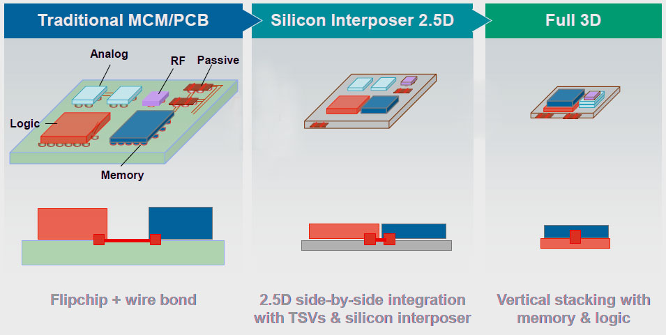
On the other hand, a 2.5D IC does not involve the stacking of dies on top of each other. Instead, the dies are placed on a silicon interposer and packaged into a single unit in a single plane. The dies are then flip-chipped onto the silicon interposer. This technology, also known as interposer technology, integrates several electronic devices inside a single package by assembling them side-by-side on a shared base.
The main difference between 3D and 2.5D packaging lies in the wiring and drilling process. In 2.5D packaging, the wiring and drilling are done on the interposer, while in 3D packaging, these processes are carried out directly on the chip to electrically connect the upper and lower chips.
While both 3D and 2.5D ICs offer significant advancements in semiconductor technology, they differ in their structural design and assembly process. The choice between the two depends on the specific requirements of the application, including factors such as power consumption, performance, and form factor.
How do 3D ICs help in Semiconductor industry?
3D integration promises to further increase integration density, beyond Moore’s Law and offers the potential to significantly reduce interconnect delays and improve system performance. Furthermore, the shortened wire length especially that of the clock net, also lessens the power consumption of circuits. 3D integration also provides a flexible way to carry out the heterogeneous system-on-chip (SoC) design by integrating disparate technologies, such as memory and logic circuits, radio frequency (RF) and mixed-signal components, optoelectronic devices, etc., onto different dies of a 3D integrated circuit (IC).
Despite the advantages, several challenges in 3D ICs need to be addressed. The most important challenge is the thermal management of a 3D IC stack due to high power density. As the number of dies in a 3D stack increases, the thermal dissipation becomes more difficult, and significant temperature drops can cause failure. Additionally, the difficulty in routing the inter-die connections increases with the number of dies due to limited space for interconnects and the increased chance of crosstalk between signals. Finally, many challenges arise in the assembly process for 3D ICs, such as die-to-die alignment, die attachment, underfill, etc.
Factors that need to be considered for 3D ICs
System-level exploration:
- Selecting appropriate silicon technology, choose the most advantageous die for optimization.
3D floor planning, placement, and routing:
- 3D floorplanner must function in the X, Y and Z direction
- Whole PD flow should be Thermal-Aware. For example:
- Moving hot blocks/cells closer to heat sinks or apart from each other
- Deliberately insert thermal vias to 3D circuits
- Thermal vias can act as a pipe that allows the heat to be conducted from the higher temp region to lower temp region
- 3D Routing of ICs must take care of wire delay due to the effect of temperature
- Critical wires should avoid hottest regions
- Interlayer vias are a valuable resource that must be optimally allocated among nets
- TSV stress, coupling and keep out areas penalty
Extraction and analysis:
- Tools must consider RLC parasitics for TSVs, micro-bumps and interposer routing
IC/package co-design:
- I/O feasibility planning, connectivity management, 3D visualization
3DIC Technology Role in AI/ML Applications
3D-IC technology has many advantages over traditional single-die planar designs. 3D-ICs are expected to have a big impact on a lot of areas, like networking, graphics, AI/ML, and high-performance computing, especially for applications that need very high-performance, low-power devices. Multi-core CPUs, GPUs, packet buffers and routers, smartphones, and AI/ML applications are some examples of specific application fields.
Advantages offered by 3DIC technology for AI/ML applications
There are many benefits are provided by 3D Integrated Circuit (3DIC) technology, which is specially designed to meet the needs of applications related to machine learning (ML) and artificial intelligence (AI):
Enhanced Performance: By stacking multiple layers of circuitry vertically, 3DICs significantly reduce interconnect lengths, minimize signal propagation delays, and improve overall performance. This increased performance is essential for speeding up AI algorithms, which frequently require intricate calculations on huge datasets.
Reduced Size and Space Saving: Compared to conventional 2D ICs, 3DIC technology enables higher degrees of integration in a smaller footprint. For AI/ML applications to be implemented in edge devices with space limits, this downsizing is crucial since it makes it possible to create small but powerful computing solutions.
Enhanced Power efficiency: Because 3D integrated circuits (ICs) can incorporate many technologies and have shorter distances between components, they also have better power efficiency. This can result in gadgets that generate less heat and last longer between charges, both of which can be crucial for meeting dependability and safety standards.
Scalability: Scalability advantages come from 3DICs’ ability to provide vertical integration, which makes it possible to integrate more computer power as needed. Because of this scalability, chipsets can keep up with changing performance requirements without compromising efficiency, which is essential given the increasingly high computing demands of AI/ML models.
These advantages are intriguing for AI/ML applications where early adoption is either about to happen or is currently taking place. For instance, big data analytics, machine learning, and artificial intelligence (AI) applications need HPC chips, which are created utilizing 3D integrated circuits (ICs). These benefits together allow for the development of incredibly robust, compact, and efficient chipsets that are capable of handling the demanding computing workloads associated with machine learning and artificial intelligence.
Conclusion
To conclude, 2.5D and 3D are the best alternatives to transistor scaling sustain Moore’s law and can achieve better throughput with an optimized area, performance<, and cost. It is most suitable for high-performance ASICs like HMCs (Hybrid Memory Cube), NAND flash, Optical sensors, and Networking ASICs.
Thus, it has become an essential part of modern chip design and is expected to play a key role in scaling in the future.
eInfochips has over two decades of experience in providing product engineering and ASIC design services on different technology nodes. It has enabled multiple Fortune 500 companies to deliver high-quality products on time.
To know more, get in touch with us.