In 1965, Gordon Moore, a co-founder of Intel, observed that the number of transistors per square inch on integrated circuits has doubled approximately every two years since the IC was invented. This is known as Moore’s law. This law has helped in the evolution of smaller, cheaper, more powerful devices, which has led to consumers taking computing technologies for granted.
As the semiconductor industry races toward lower-technology nodes, the focus now is on more powerful chips with a reliable Internet of Things (IoT) support. Considering this, the IoT has become a mainstream technology for companies looking to accelerate the growth of chip connectivity in the upcoming years.
Moreover, with the emergence of the IoT, the semiconductor industry has an opportunity to use Moore’s law to deliver computing capabilities that can support Internet-connected devices like desktops, smartphones, and wearables. This allows interconnections between different kinds of ecosystems and creates three major requirements for electronic design automation (EDA) companies: lower geometry design, low power dissipation, and low cost.
If you pay attention to the emerging changes in the semiconductor industry, you will notice that the market has seen a continuous discussion about tape-out on 16-nanometer and 10-nanometer lower geometries, even hitting the 7-nanometer wall and beyond for developing high-performance systems after only a few days. With regard to this ongoing trend of diminishing transistor geometries, engineers are struggling to find a way to manage the difficulties inherent to lower-technology nodes. Some common challenges engineers face are as follows:
Chip Size
Companies are increasingly facing the challenge of reducing the sizes of transistors and technology nodes without affecting the performance of chips in order to meet the consumer demand for IoT products. Chip manufacturers, therefore, are looking for IoT components that are as small as possible, which results in good RF performance and affordability.
Power Dissipation
Power consumption analysis and management have also become critical for chip manufacturing companies. As the IoT continues to expand and becomes the next frontier of technology in the coming days, the new range of applications demands power minimization, which is one of the major challenges with small transistors in getting the best performance out of IoT applications and devices. The power consumption in a chip can be divided into three major categories: dynamic power, short-circuit dissipation and leakage power dissipation.
Security and Privacy
Chip manufacturers believe that if the IoT is ever going to truly take off, it will create security and privacy problems. The 2015 Icontrol State of the Smart Home study found that 44 percent of all Americans were very concerned about the possibility of their information being stolen from their smart home, while 27 percent said they were somewhat concerned about the security of chip implementation. Such security concerns have been addressed by a few companies; however, the prime challenge is to prevent any theft of information by building required security measures into applications and network connections.
Testing to Enhance Performance
As the size of a transistor is reduced, this gives rise to solid-state drive (SSD) fault defects. Thus, it becomes difficult for companies to diagnose defects on a frequent basis, identify the suitable design-for-test (DFT) techniques, and reduce costs and time-to-market so as to power up the performance of chips.
Wire Interconnecting Delay
As chip size shrinks, engineers face challenges in scaling wire length. In addition, it becomes difficult in the case of fine-pitched wires to leverage lower-design technology density and limit complexity. Thus, challenges of scaling and interconnectivity between wires limit the performance and connectivity of devices in the IoT ecosystem.
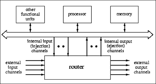
Due to a continuous reduction in lower-geometry design, the semiconductor industry follows architectural and node-processing-based techniques in developing and implementing new nodes. The architecture-based technique upgrades a new set of processors, based on micro-architecture for large performance upgrades. The node-processing-based technique consists of a switch, a buffer and other functional units (see Figure 1).

There are other suites of services, like Netlist to GDSII, Sign-off, Design for Testability, ATPG Challenges and Double Patterning in lower-technology nodes, which can enable service providers to address advanced fabrication process and ensure the right quality of silicon, every time. With this in mind, it’s vital to consider how the IoT relates to Moore’s law and challenges faced by the semiconductor industry to scale IoT applications.
eInfochips has over two decades of experience in providing product engineering and ASIC design services on different technology nodes. It enables multiple Fortune 500 companies to deliver high-quality products on time. To know more, get in touch with us.
Know more about


