In the ever-evolving landscape of electronic engineering, the Land Grid Array (LGA) has emerged as a pivotal solution, deftly addressing the contemporary demand for compact yet potent systems. At its core, the LGA encapsulates the convergence of cutting-edge semiconductor technology and meticulous packaging design, offering a compact housing for formidable System-on-Chip (SoC) units while accommodating their voracious power appetites. Positioned as a direct mountable solution on Printed Circuit Boards (PCBs), the LGA epitomizes efficiency, enabling the realization of high-performance devices within confined spatial constraints.
In this blog, we explore what the Land Grid Array (LGA) is, the technology behind it, its applications, its importance in embedded electronics design, and the testing methodologies involved.
What is Line Grid Array (LGA)?
- Line Grid Array is a design technology that allows for the placement of major components like microprocessors, memory, RF sections, and power management sections on one side of the PCB, while the other side features a grid of pads.

LGA packages are eye-catching due to their impressive pin density (number of pins), compact design, and superior thermal performance.
- In certain high-density boards, Low Side Capacitors (LSCs) are sometimes located on the underside of the PCB.
When designing a final product, an LGA package can be directly mounted to a base, interposer, or carrier board using solder paste. However, during the development phase or when testing multiple LGA variants that share the same form factor on the same processor/CPU, it’s preferable to use a socket for mounting the LGA package.
Due to their strong and reliable connections, LGA packages are widely used in the embedded and semiconductor industry.
1. System on Module (SOM)
- LGA SOM packages have become popular due to market demand and space constraints for high-end processors and CPUs.
2. Chipsets
- Chipsets, which facilitate high-speed or low-speed communication between various components and integrated circuits on a PCB, require durable and reliable connections.
3.Networking and Radio Frequency
- LGA technologies find applications in 5G, 4G, and other bandwidth-intensive networking technologies like IoT, NB-IoT, Zigbee, Wi-Fi, and BT modules.
There are numerous applications that are using the LGA technologies. Listed below are a few applications that have adopted the LGA technology. Design consideration of LGA for System on Module (SOM):
1. Footprint/Land pattern of LGA module
- Customizable footprints with carefully chosen pad sizes and pitch distances contribute to increased yield rates.
- When designing LGA modules, it is important to consider the size of the LGA pads and their pitch. As a general rule of thumb, the pad pitch should be equal to or greater than twice the size of a single pad. For example, if the pad size is 0.7×0.7mm, the recommended pitch would be 1.4mm. However, depending on the capabilities of the PCB fabricator and the complexity of the design, designers may have some flexibility to adjust the pad pitch within certain limits.
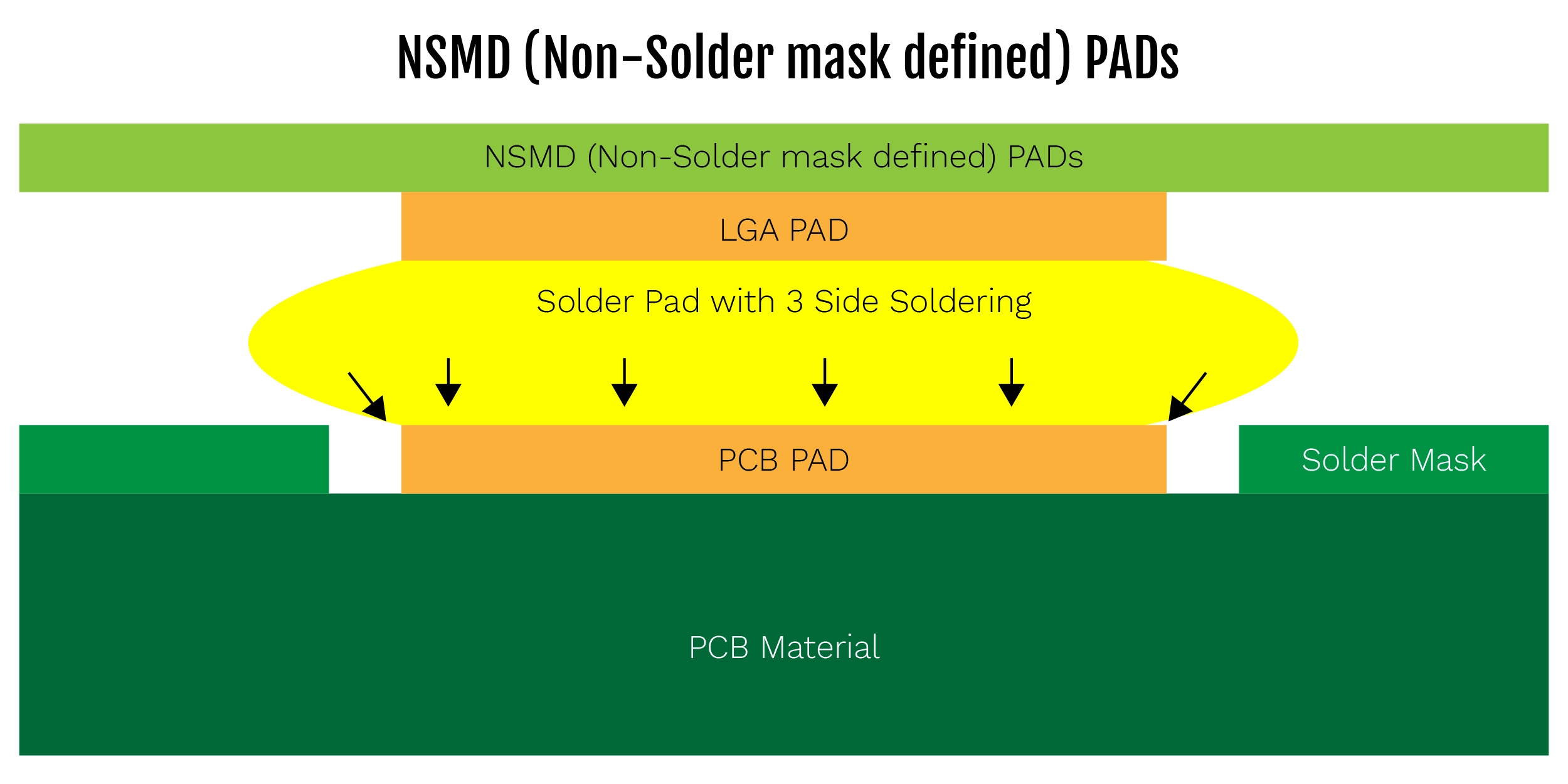
- Non-Solder Mask Define (NSMD) pads are recommended to escape the voids in solder joints between LGA module and carrier board. NSMD pads have a solder mask opening that is smaller than the actual coppe r pads.

2. Assembly and conductivity
- LGA modules enable the use of Electroless Nickel Immersion Gold (ENIG) as a PCB surface finish, improving solderability and minimizing void areas in pad assemblies.
- It also helps prevent corrosion during storage and soldering.
3. Carrier Board/Interposer board design
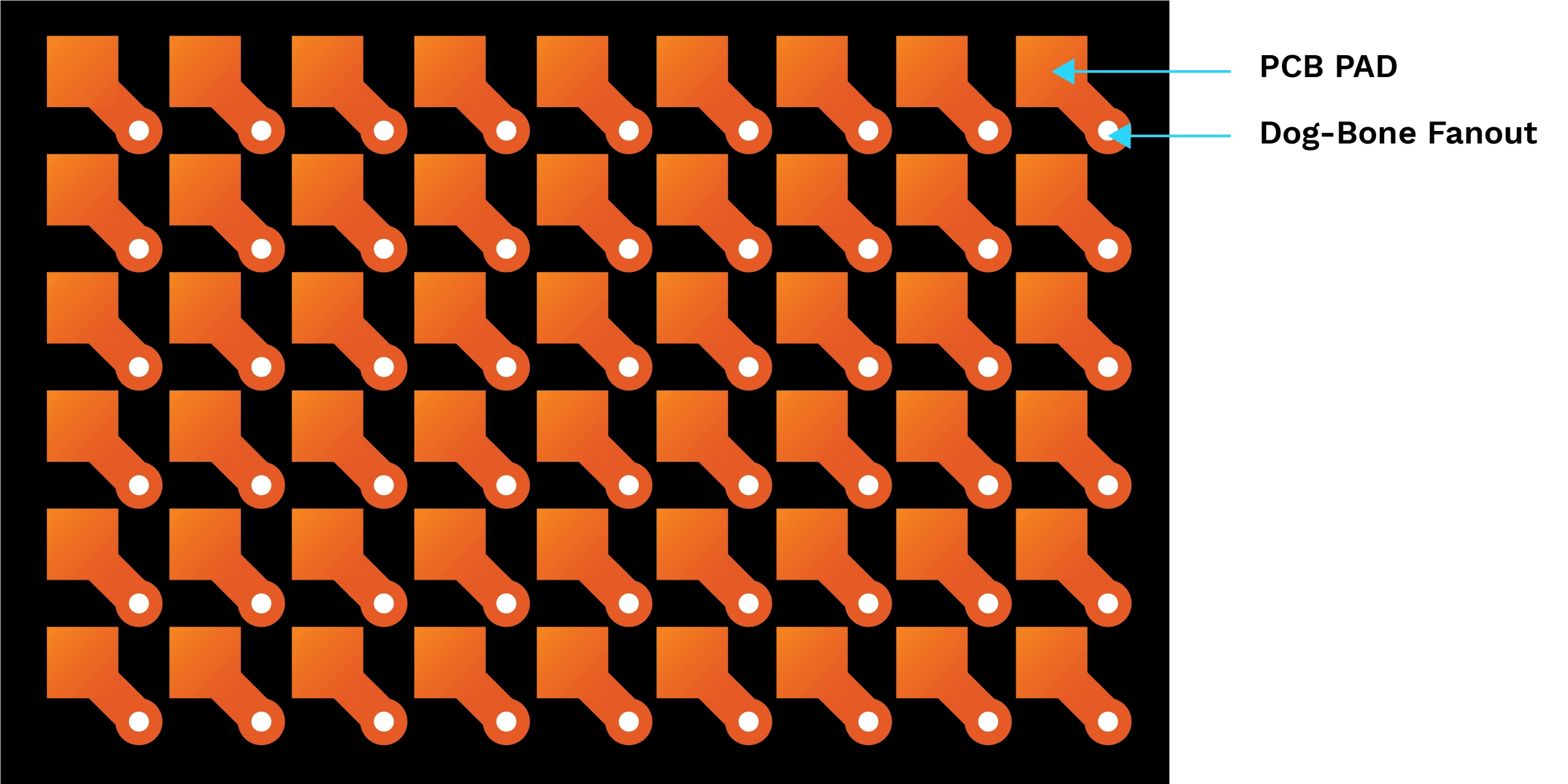
- Designers can leverage the flexibility of pad sizes and pitches in LGA module design to simplify and reduce the cost of carrier board design. Optimal LGA pad pitch can be used for Through-Hole (TH) dog-bone routing design, reducing fabrication costs.
- Constraints of drill size should be considered when planning the dog bone in TH designs.

4. Power Delivery Network (PDN) of LGA Module
- Designing a highly dense PCB around a processor with multiple power rails and PMICs requires careful consideration of the PDN.
- Achieving the desired Direct Current Resistance (DCR) can be done with minimal effort by ensuring a substantial power shape area from the power source to the delivery point. However, as the frequency increases, challenges may arise in managing impedance peaks (ZPK1, ZPK2), impedance, and inductance, particularly at 200MHz.
- Low DCR feedthrough capacitors (3-pad capacitors) can be utilized to meet high-frequency impedance and inductance requirements.
5. Stencil design for LGA carrier board
- Stencil thickness:
- To minimize solder void areas, a stencil thickness partially stepped up to 0.125mm-0.150mm is recommended.
- As per recommendations void area should be less than 30% (this can vary based on assembly house capability).
- Recommended to use type IV/V paste material for the assembly.
6. Reflow profile for LGA carrier board
- General reflow profiles can be used for LGA modules, but they can vary depending on the carrier PCB and the LGA module components.
- Soak time (150°C–190°C): 60 s–70 s
- Ramp time (190°C–220°C): 20 s–25 s
- Peak temperature (minimum 245°C): Temperature measured on body of part.
- Time above liquidus: 45 s–70 s
Note: The use of nitrogen is recommended to assist solder wetting

LGA Testing methodology
- LGA module testing is a critical aspect of the design process, and there are various testing methodologies available from different vendors.
- Socket design is the most common testing method, but other technologies like PCBeam and pogo pin type sockets are also used.
- PCBeam technology offers different pad pitch options – 0.65 mm,0.8mm, 1.0mm, and 1.27mm, and has up to a hundred cycles to test the module.
- Another technology option is POGO pin technology that enables the connection between the LGA module and interposer board through a POGO-pin based socket. With this setup, all pins of the LGA module can be conveniently connected to the interposer board.
- Pogo pin-based solutions offer the advantage of any pitch, making them advantageous for dense boards, although they come at a higher cost.
Summary
The blog explores Line Grid Array (LGA) technology, its applications, and design considerations. LGA packages offer high pin density, compact design, and improved thermal performance. They are widely used in embedded electronics, chipsets, and networking. Design considerations include customizable footprints, optimal assembly and conductivity, simplified carrier board design, and proper power delivery network. LGA testing methods include socket design, PCBeam, and pogo pin technologies.


