Nowadays, placing multiple IPs on a single chip plays the most vital role in satisfying System on Chip ASIC specification requirements. Most of the time, these different IPs will have different clock domains.
In this scenario, the use of multi-clock domains is becoming vital in elaborate designs for balancing scan chains as a limitation to Scan I/O ports. Majorly, in DFT, we avoid mixing different clocks in the same chain, but if there is a constraint to I/O ports we have to stitch scan flops driven by two different clocks in one chain. However, such a scenario will be an invitation to challenges like hold violations and generating patterns for transition delay fault to cover faults between clock domains.
DOWNLOAD CASE STUDY
Design for Testability for a High-speed Gigabit Ethernet Controller for Networking
This article presents usage of lock-up latch and a delay test concept for SoC devices with multiple clock domains. Circuitry for high-speed on-chip clock generation is implemented in SoC to avoid expensive test equipment. The usage of an ATE for clocking also requires a high-speed clock generator to apply at-speed clock pulses for launch and capture. Usually, such a high-speed clock generator is not available in low-cost ATE.
DFT Challenges
Now, let us talk about DFT challenges for multi-clock domain design. Using mixed clock in the same scan chain would lead to:
- Hold violation
- Coverage drop during the transition-delay-ATPG (Automatic Test Pattern Generator)
Let us understand these two challenges in brief:
1) Hold time violation
Hold Time: The minimum amount of time after the arrival of clock edge in which the data needs to be stable is called ‘hold time.’ In other words, the data needs to be stable for some time after the arrival of clock edge so that the data can be captured properly. A violation in this case may cause incorrect data to be latched, which is known as a hold violation.
We know that the data to be captured at the current clock edge was launched at the previous clock edge by some other flip-flop, while the data launched at the current clock edge must be captured at the next clock edge. Hold time takes care that the data launched at the current clock edge is not captured at the current clock edge and the data launched at the previous clock edge is captured and is not disturbed by the one launched at the current edge. Hold time ensures that the current state of the design is not disturbed.
2) Coverage drop during the transition-delay-ATPG (Automatic Test Pattern Generator)
RELATED BLOG
SoC devices implement multiple functional clock domains. An at-speed test has to test all clock domains at their own functional speeds. In such a case, the solution is that the testing should happen on one clock domain after another for multi-clock domain delay test.
While doing this, it generally happens that the logic between such clock domains remains untested, with a penalty in terms of increase in pattern count and reduced coverage. Achieving high fault coverage during test proves to be one of the biggest DFT challenges for designs with multiple clock domains.
Approach to Fix DFT Challenges
1) Overcoming Hold Violation
To overcome Hold Violation let us explore the below scenario:
If all scan cells receive a clock edge at the same time, no timing violations occur. However, if a different clock domain is used because of latency in clock domain, hold violations may occur.
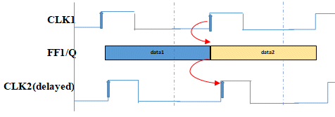
Consider an example of two scan flops driven by two different clocks.

If the CLK2 waveform at FF2 is delayed, a hold violation might result where FF2 incorrectly captures the current cycle’s data instead of the previous cycle’s data. Fig. 2 shows this hold violation for leading-edge scan cells.
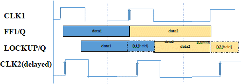
A lock-up latch prevents hold violations for scan cells that might capture data using a skewed clock edge. It is a latch cell that is inserted between two scan cells and clocked by the inversion of the previous scan cell’s clock. Fig. 3 shows the same two scan cells with a lock-up latch added.

The lock-up latch cell works by holding the previous cycle’s scan data while the current cycle’s scan data is captured, effectively delaying the output data transition to the next edge of the source clock. Fig. 4 shows the lock-up timing behavior for the example.
2) Coverage drop during the transition-delay-ATPG (Automatic Test Pattern Generator)
The solution to this issue is ‘Synchronous OCC’ technique. Let’s dive deeper into it.
The technique of synchronous on-chip clock generation is meant to reduce the test vector count and to increase test quality. A synchronous OCC can generate clock pulses between each synchronous clock domain that goes through the OCC (one pulse per domain) to cover faults between the clock domains. The OCC shift chain bit values are used to generate the targeted clock pulses (launch and capture) for each clock domain.
Fig. 5 below shows a scenario where synchronous OCC sync two different clocks for generating the pattern of transition-delay fault model.
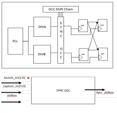
Here, launch_en [1:0] is indicating launch bit from 2 different OCC similarly for capture_en[1:0]. By applying constant 1 value to the shiften, we can get launch and capture pulses from pulse shaping circuit based on launch and capture bit.
DFT Tool – DAeRT : Dft Automated execution and Reporting Tool
DAeRT enables to achieve ~100% testability for the ASIC designs. It supports various DFT methodologies starting with IJTAG/JTAG, MBIST, Scan, ATPG, Pattern Validation, Test Timing Analysis and Post-Si validation.
How Sync OCC works
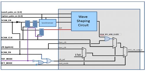
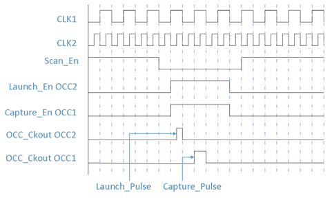
Basically, Sync OCC is used to generate launch and capture pulses from two different clock domains during the capture operation, as shown in Fig. 6.
Let us see this in detail:
- Apply value 1 to TDF_MODE and DFT_MODE. Now clk_sel will be dependent on SCAN_EN. So if SCAN_EN=1 (Shift operation), it will select SCAN_CLK while SCAN_EN=0 (Capture operation), it will select func_clk.
- Now let’s consider SCAN_EN=0 for capture operation. After two clock cycles of SCAN_CLK, it will drive the synchronizer circuit.
- Here Launch_pulse_en[0] and Capture_pulse_en[0] are related to OCC-1 while Launch_pulse_en[1] and Capture_pulse_en[1] are related to OCC-2.
- The synchronizer circuit will generate 1 value on Launch_pulse_en[0] and Capture_pulse_en[1] in such a way that the output of Wave Shaping Circuit is 1 for two functional clock cycles.
- As SCAN_EN=0, TDF_MODE=1, and DFT_MODE=1, we will get launch pulse and capture pulse as output on OCC_clk_output.
Please check the waveform shown in Fig. 7
ATPG Setup
1. Write Clocking Procedure for Sync OCC
Consider a design having 71 OCC. In such a case, OCC shift chain contains 142(71*2) flip-flops (here 2 represents launch bit and capture bit of each OCC). The clocking procedure for it will be:
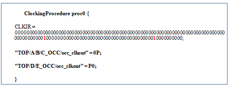
In this example, CLKIR has 142 bits; by setting it to 1, we can get launch and capture pulses from respective the OCC.
Based on CLKIR sequence, we can get launch pulse from E_OCC and capture pulse from C_OCC.
2. Add the below command TMAX script

Conclusion
For next generation ASICs SoC having multiple IPs functioning at different clock domains, the on-chip clock generation circuit plays a key role. The methodology described in this article helps to improve fault coverage with the minimum pattern count. It also helps in assuring on hold violation check as we can confirm one cycle delay between launch and capture pulse.
Build your next-generation SoC with DFT engagement model
Authors
Ramesh Devani, Mayank Kapadiya, Piyush Chaniyara and Khushali Dudhagara


