While developing large-sized chips, “divide & conquer” techniques are used. This involves partitioning the design, implementing each block individually, and stitching them together at the top level. Even if the blocks are all clean with respect to physical design and timing signoff, they show incremental violations when they are stitched together.
These violations come primarily on interface nets – nets which are interfacing other blocks or other cells at the top level. One of the primary physical design checks is the antenna, which can damage the gate and subsequently lead to functionality malfunctions on the chips. While implementing the block, individual blocks would not be aware of other geometries/net length which are coming from the top level or interface blocks.
When the chips are large in size, comprising of multimillion instances and multiple partitions, the execution time for running all signoff checks at the top level will have a huge penalty on run time and will also increase the number of signoff iterations at the top level required to make it all clean. Every signoff iteration at the top level and then fixing violations at the block level will have multiple back and forth loops to close the IC (ASIC) design and this can increase the time to market.
DOWNLOAD CASE STUDY
Physical Design of a 7nm based Superfast Programmable Ethernet Switch ASIC
For checking antenna violations, we need to evaluate the cumulative metal area ratio to the active poly gate area. Running antenna checks at the block level will help obtain correct information of the gate area, but will miss the information on the actual metal area, which is outside the block.
If we can give metal area information, which is connected to the respective gate, then we can accurately determine the antenna violations and fix them at the block level. All the block level internal antenna violations are taken care of during the rf block level signoff quality checks. This approach is primarily used for identifying the gates, which are connected to block ports.
If we can extract all full chip geometries or interface nets geometries from other blocks and provide that information at the block level, we can accurately find the antenna violations and fix at the block level. As this approach is a miniscule version of the full chip antenna run where all non-significant geometries are removed, we will cut down on the full chip run time but at the same time will get all violations at the block level.
Traditional approach
Traditionally, a two-step process is used to get the valid antenna ratio:
Step 1
Antenna at block level: This step extracts metal vs. poly gate area ratio for all the shapes residing in the block. But it is missing the real ratio of geometries stitched to interface poly gate.
Step 2
Antenna at full chip designing: This step helps in finding the real antenna ratio connected to boundary gates.
To report the true effect of antenna from the full chip run, we need to:
- Merge all individual blocks with full chip and output the large size Oasis.
- Physical design Verification tool extracts the merged top level IC design and looks for violations based on the rule defined from the foundry.For a large size chip, this step takes a long run time (more than a day or so) to deliver the violations.
- Finally, based on the results, the individual block owner is asked to clean the reported violations found (if any) over the block.
Antenna violations can be fixed by adding a diode for increasing the gate area, or by applying layer hopping for reducing metal area. For boundary net’s antenna violation, there is always a dependency on the next full chip signoff cycle, because at the block level these cannot be verified after applying local fixes.
What if the applied solutions are not sufficient to get rid of the reported violations? Then it’s another push for the block owner to put an incremental fix and again wait for the full chip antenna run. Therefore, this process takes a longer turnaround time to make the database all clean for the fabrication process.
Please note that antenna checks are performed parallel to signoff checks, along with the feedback on timing/noise/DRC provided by the top level. As a result, they can cause some changes in connected interface/full chip geometries, which might trigger an antenna violation if the metal to gate area ratio is changed.
Suggested Approach
To receive true antenna information, we should have all geometries in existence along with the gate connected to it. However, while at the block point of view, metal shapes connected to interface poly gate are missing.
If we can involve connected metal shapes to interface poly gates, then we can manage to get the actual antenna ratio in the block level itself. These metal shapes could be connected to the top level or with the neighboring blocks.
To understand the concept in detail, please see the chip level floorplan below, which shows all the interfacing blocks/cells for nets in Design A.
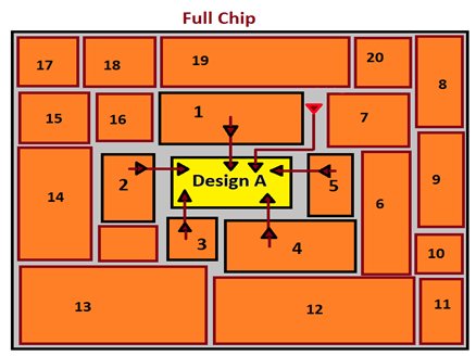
In Figure 1, Design A has some input gates, which are getting driven by neighboring blocks and full chip cells.
In this case, neighboring blocks and full chip metal geometries should be involved to calculate the total metal area for boundary poly gates. This way, the actual metal to gate area can be calculated.
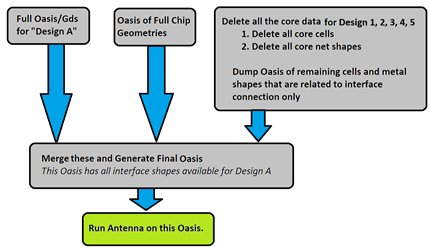
Figure 2 highlights the suggested approach that can be used to boost up closure of Antenna. This method requires two steps:
Step 1
- Full Oasis of Design A: This will have complete physical design information, including interface poly gates, for the specific IC design.
- Oasis of full chip designing: Oasis for full chip should have all the geometries and poly gates available at the top level. Even for large size chip, This Oasis, is not going to be heavy in size.
- Oasis of neighboring blocks: These Oasis should be having only interface metals and poly gates. To generate this file, it is required to delete all the core cells and net geometries. This step, again, doesn’t take more than 15 minutes for a million instance design.
It is recommended to use interface Oasis for neighboring blocks. Also, this step is for analyzing metal to gate ratio for Design A; so, taking complete Oasis is unnecessary and it increases run time by more than 2.5X.
Step 2
Generate final Oasis by merging all these files, which will have all the required information for getting the true antenna ratio for Design A. This should be input file that is used for launching the antenna run.
Now, the results reported by physical verification tool include everything for Design A. Therefore, cleaning up these violations makes sure that we don’t see any surprises during the full chip antenna run for Design A.
This method takes almost the same amount of run time that an individual block level antenna run takes. In addition, we are able to replicate all the related antenna violations to the specific design that should have been caught during the full chip antenna run.
Experimental Data
We deployed this method in one of the projects that we were working on. When we used this method, all antenna violations at boundary nets in the block level runs correlated to all antenna violations which are reported in full chip runs. As all violations are now visible at the block level, they are easy to get fixed and validated at the block level runs and this also reduces multiple iterations for the top level runs.
Here are some data points for one of the million instance designs.
| Block Level runtime of Design A | 50-60 minutes |
| Generation of Interface shapes oasis of neighboring designs |
15-20 minutes |
| Suggested Method runtime of Design A |
90-120 minutes |
| Top Level Antenna runtime | More than 22 hours |
| Violation Count for Design A | Matching to full chip antenna report |
As mentioned, the runtime of Design A was not high with the given approach, and we were able to validate all the fixes applied for improving the antenna ratio for Design A.
To make this step easier, we developed a scripted flow for creating interface Oasis of neighboring blocks and for generating final Oasis after merging. To make all pre-requisites available, we dumped all the required information of all neighboring blocks, while releasing blocks at the central area. This area always gets an updated Oasis file if there is any update in any design.
Advantages
- This approach is very beneficial for large ASIC chip sizes design. Traditionally, we are dependent on the full chip antenna run to confirm applied solution. For run time intensive large chips, it is not possible to get an updated full chip antenna report as and when the individual block requires.
- This is a truncated version of the full chip antenna run, but helps in faster IC design closure from the top level point of view.
- A big advantage is reducing the run time and reducing signoff cycle at the top level.
- Helps in reporting all the real antenna ratio for interface geometries as well.
- Individual block owners can validate all deployed solutions at the block level.
- Incremental fixes can be applied and validated. So it doesn’t require you to wait for another full chip antenna drop to confirm applied fixes.
Conclusion
This is an effective alternative technique for the quick fixing of full chip antenna violations at the individual block level itself. The reported antenna results with this technique are the same as a full chip antenna run, but the execution time of this approach is much faster than the traditional method. Using this method can be very helpful in reducing signoff iterations for the top level antenna. For more information, you can refer to this tweaker in VLSI.
Accelerate timing and power signoff iterations in your SoC design
